1 Hardware
1.1 Installation
The Ndigo6G-12 board can be installed in any PCIe x8 (or higher amount of lanes) PCIe slot. If the slot electrically supports less than eight lanes, the board will operate at lower data throughput rates.
Connect a 6-pin PCIe power cable to the connector at the rear of the board (see Figure 1.1). When using an external 12 V power supply, be aware that it must be switched on before you boot the host system of the Ndigo6G-12. Note that when you power cycle the host system without power cycling the external 12 V power supply, the Ndigo6G-12 will not power cycle. This should generally not be a problem, unless you were to perform a firmware update.
Note
The Ndigo6G-12 does not operate without a 6-pin PCIe power connector.
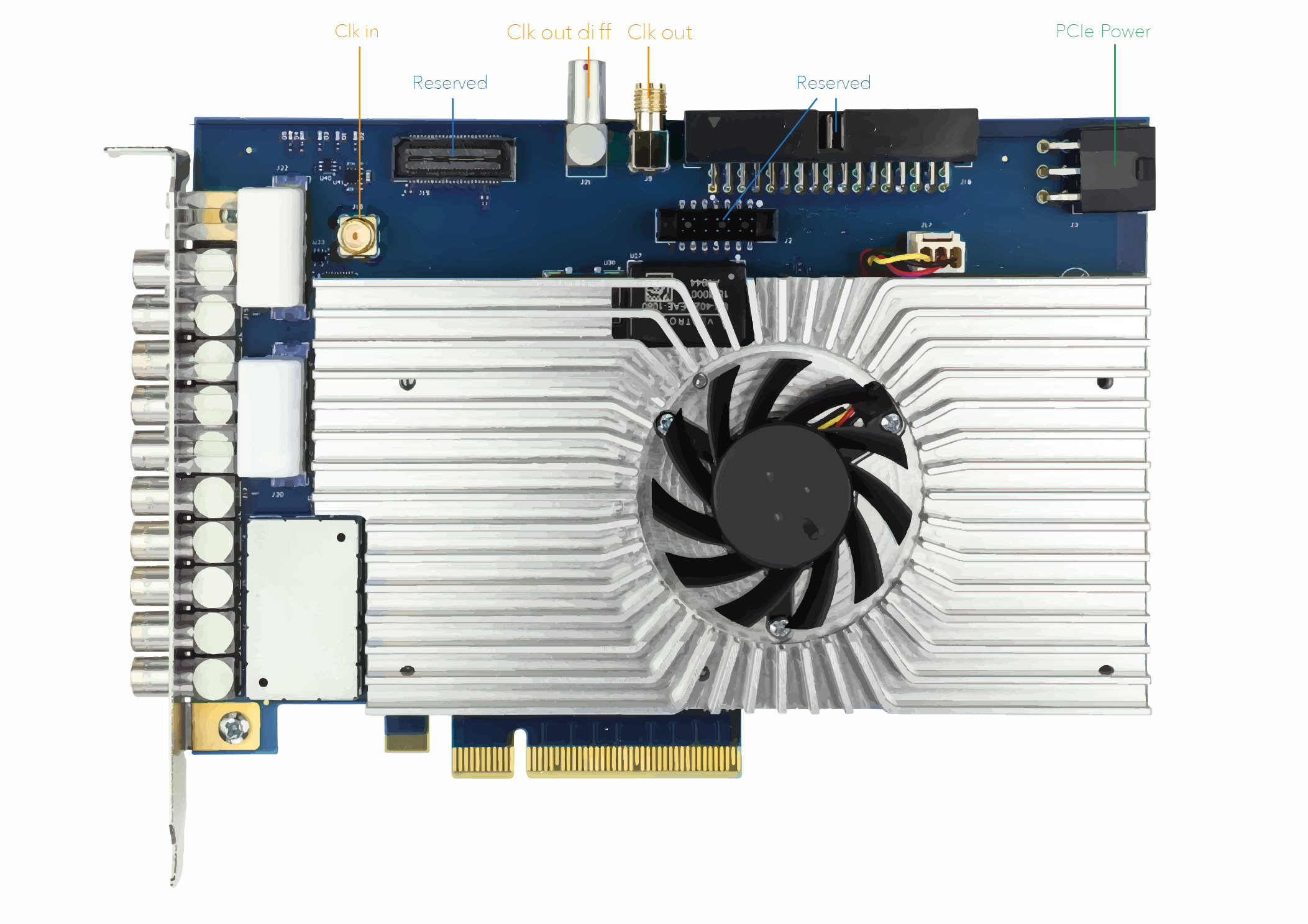
Figure 1.1: Overview of an Ndigo6G-12 board. Note the PCIe power connector at the rear of the board.
1.2 Cooling
The Ndigo6G-12 board is equipped with an active cooling system, ensuring proper cooling of the device. If, however, the temperature of the ADC, TDC, or FPGA chips on the board exceed critical temperatures (for instance, if the device is operated in inappropriate environmental conditions, see Section 6.3.1), a warning is issued to the device driver.
The temperature warnings can be read out using
ndigo6g12_fast_info::alerts.
1.3 External Inputs and Connectors
1.3.1 Front bracket inputs
The inputs of the Ndigo6G-12 board are located on the slot bracket.
Figure 1.2 shows the location of the four analog inputs A to D (see Section 1.3.3), the four digital TDC inputs 0 to 3 (see Section 1.3.4), and the two digital control inputs TRG and GATE (see Section 1.3.5).

Figure 1.2: Input connectors of an Ndigo6G-12 board located on the PCI bracket.
1.3.2 Clock connections
Connectors to connect an external clock or to access the internal clock signal are located at the top of the board (see Figure 1.1).
- Clk in (SMA)
Connect your external 10 MHz clock signal here. Make sure to set
ndigo6g12_init_parameters::clock_sourcetoNDIGO6G12_CLOCK_SOURCE_SMA.- Clk out (SMA)
10 MHz output. This is either the internal clock signal, or an external clock 10 MHz clock if one is used.
- Clk diff (LEMO00)
Same as Clk out, but as a differential signal and with a LEMO00 connector.
1.3.3 Analog Inputs

Figure 1.3: Input circuit for each of the four analog channels.
The analog inputs of the ADC are single ended LEMO00 coax connectors. The inputs have a 50 Ω impedance and are AC coupled. The inputs are converted to a differential signal using a balun.
Analog Offsets
AC coupling removes the DC voltage offset from the input signal.
However, users can shift the DC baseline voltage before sampling to a value of
their choice (using the
analog_offset
parameter).
This feature is useful for highly asymmetric signals, such as pulses from TOF spectrometers or LIDAR systems. Without analog offset compensation, the pulses would begin in the middle of the ADC range, effectively cutting the dynamic range in half (see Figure 1.5). By shifting the DC baseline to one end of the ADC range, the input range can be used fully, providing the maximum dynamic range. The analog offset can be set between \(\pm\) 0.5 V.

Figure 1.4: Users can add an analog offset to the input before sampling.

Figure 1.5: Asymmetric signal shifted to increase dynamic range.
AC-Coupling and Baseline Drift
Due to the AC-coupling of the analog and digital inputs, a baseline drift may occur over time (see Figure 1.6). To avoid this problem, make sure your input signal fulfills the requirements laid out in Section 6.3.4.

Figure 1.6: Baseline drift due to AC-coupling. A second pulse close to a first may be influenced by a shifted baseline, as sketched in the lower graph.
1.3.4 Digital TDC Inputs
The Ndigo6G-12 board includes four TDC channels with 13 ps timing resolution. The inputs are AC coupled (see Figure 1.7).

Figure 1.7: Principal input circuit for each of the digital TDC and control inputs.
The following members of the ndigo6g12_configuration struct
configure, respectively, TDC channels 0 to 3:
tdc_trigger_offsets[0:3]Configure the DC offset.
trigger[NDIGO6G12_TRIGGER_TDC0:NDIGO6G12_TRIGGER_TDC3]Configure if an edge or level trigger is used (relevant, if the TDCs are used in
trigger_blocksorgating_blocks) and if the rising or falling edge of the input signal triggers.tdc_configuration.channel[0:3]Configure if (
channel[0:3].enable) and when (channel[0:3].gating_block) timestamps are recorded on the TDC channel.
The trigger unit input logic is summarized, as well, in Figure 2.14.
1.3.5 Digital Control Inputs
There are two digital control inputs on the front slot cover called TRG and GATE.
TRG and GATE can detect pulses with a width that is least 2 ns and at maximum 200 ns.
Input-signals on the inputs TRG and GATE are digitized and routed to the Trigger Matrix. They can be used to trigger any of the trigger state machines and gating blocks with maximum sampling rate.
The digital control inputs are optimally suited to be used as digital triggers and gates, and we recommend using them instead of the digital TDC inputs for these purposes.
TRG and GATE are configured analogously to the TDC inputs (see
Section 1.3.4 and
Figure 2.14), where indices 4 (5) and
NDIGO6G12_TRIGGER_TRG (NDIGO6G12_TRIGGER_GATE)
correspond to input TRG (GATE).
The input circuit and trigger logic is identical to the TDC inputs (see Figures 1.7 and 2.14).
Use Control Inputs as TDCs
The control inputs TRG and GATE can be used as low-resolution TDCs. The dead-time is 5 ns. Pulses should have a width of at least 300 ps to reliably be detected.
Hint
To record timestamps with the TRG or GATE input, set
config.tdc_configuration.channel[4||5].enable
to true.
Note
The digital control inputs TRG and GATE are best suited for triggering and controlling gates.
The digital TDC inputs are best suited for measuring precise time stamps.
1.4 Memory management
The host buffer is memory on the host’s system in which the data recorded by the Ndigo6G-12 is stored until it is acknowledged by the user.
The host buffer is managed by the DMA (direct memory access) driver. The DMA driver can only ever write to the host buffer if enough memory is free. That means, new packets will never overwrite old packets, unless they have been acknowledged.
If the host buffer is full, data may be lost.
Then, the CRONO_PACKET_FLAG_HOST_BUFFER_FULL bit of
crono_packet::flags is set.
To ensure that this does not happen, the user must acknowledge packets
fast enough by the analysis software.
Note that data only has been lost due to a full host buffer if the
CRONO_PACKET_FLAG_TRIGGER_MISSED bit of crono_packet::flags
is set.
1.4.1 Acknowledge Packets
A packet in the host buffer will only be overwritten if it has been acknowledged.
This can be done manually by the user by calling
ndigo6g12_acknowledge() or automatically by the driver if in the call of
ndigo6g12_read(), in.ackwnoledge_last_read of
was set to true.
Acknowledging a packet acknowledges all previous packets as well.
Be aware that acknowledging a packet immediately invalidates it, and it is unsafe to attempt accessing its content.
1.4.2 Internal Memory Layout
The Ndigo6G-12 uses internal FIFO (first-in, first-out) memories.
In one of these FIFOs, referred to as the DMA
FIFO, packets that are ready to be sent to the host system are buffered.
If the DMA FIFO is full at any point, the affected packets
CRONO_PACKET_FLAG_DMA_FIFO_FULL bit of crono_packet::flags
is set. This does not mean that data has been necessarily lost. Only if the
CRONO_PACKET_FLAG_TRIGGER_MISSED bit is set has data been lost.