Hardware
Installing the Board
The Ndigo5G board can be installed in any x4 (or higher amount of lanes) PCIe slot. If the slot electrically supports less than four lanes, the board will operate at lower data throughput rates.
Please ensure proper cooling of the device. The Ndigo5G has an onboard temperature detection. If the ADC chip temperature exceeds 90° C, a warning is issued to the device driver. In case the temperature is higher than 95° C, the ADC is disabled to avoid damage. Using a PCI-slot cooler is in many cases an appropriate solution to circumvent problems caused by overheating if the board is used inside a PC. The Ndigo Crate will provide sufficient cooling under normal operating conditions.
Using a single Ndigo5G, no further connections need to be made. For applications that require more than four ADC channels, several Ndigo5G boards can be operated in sync.
Attention
In some cases, modern PC mainboards have PCIe slots with an additional metal shielding. Be careful not to cause an electric short when installing the board as some board components are located close to the PCIe connector.
The signals used for board synchronization and inter-board triggering are transferred on a bus between the boards. Join all C2 connectors (see Figure 1) on the boards using a ribbon cable. Both ends of the bus need to be terminated properly. If using a Ndigo Crate, connectors providing the termination are located on the crate mainboard next to the PCIe slots to the extreme left and right. For more details, please refer to the Ndigo Crate user guide. In applications that use only a few Ndigo boards installed directly inside a PC, termination PCBs that available from cronologic can be used.
Ndigo5G’s standard device driver can be used to read out all boards and acquire data. For more complex scenarios, using the cronoSync library, which is part of cronoTools, is recommended. The cronoSync library is provided with the Ndigo device driver. Please refer to the cronoTools user guide for more information.
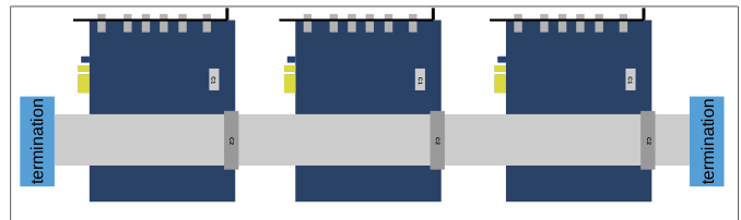
Figure 1 Principle setup for connecting several Ndigo boards to work in sync. The boards must be connected using a ribbon cable as bus for synchronization and trigger signals. At both ends of the cable, proper termination is required.
External Inputs and Connectors
Connectors
The inputs of the Ndigo5G are located on the PCI bracket. Figure 2 shows the location of the four analog inputs A to D and the two digital inputs G (GATE) and T (Trigger). Furthermore, two board interconnection connectors can be found at the top edge of the Ndigo5G, as shown in Figure 3.
Connector C1 is used for a board-to-board connection (e.g., to link a HPTDC8-PCI and a Ndigo5G via a Ndigo Extension board, see Extension Card).
Connector C2 is used as a bus interface between multiple Ndigo boards distributing clock, trigger and sync signals. It can be used to supply the Ndigo5G with an external 10 MHz clock or to output such a signal (depending on the initialization parameters, see Initialization).
Refer to Table 1 for the pinout. Proper termination must be placed at both ends of the bus interconnection ribbon cable.

Figure 2 Input connectors of an Ndigo5G located on the PCI bracket.
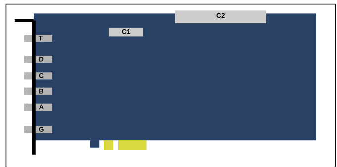
Figure 3 Schematics of an Ndigo5G board showing inter-board connectors C1 and C2.
Pin |
Name |
|---|---|
1, 2 |
GND |
3, 4 |
ext. CLK in (or out) N, ext. CLK in (or out) P |
5, 6 |
GND |
7, 8 |
reserved/NC |
9, 10 |
GND |
11, 12 |
reserved/NC |
13, 14 |
GND |
15, 16 |
reserved/NC |
17, 18 |
GND |
19, 20 |
reserved/NC |
21, 22 |
GND |
23, 24 |
reserved/NC |
25, 26 |
GND |
27, 28 |
reserved/NC |
29, 30 |
GND |
31, 32 |
reserved/NC |
33, 34 |
GND |
Analog Inputs
The analog inputs of the ADC are single ended LEMO00 coax connectors, the circuit of which is shown in Figure 4. The inputs have a 50 Ω impedance and are AC coupled. The inputs are converted to a differential signal using a balun.
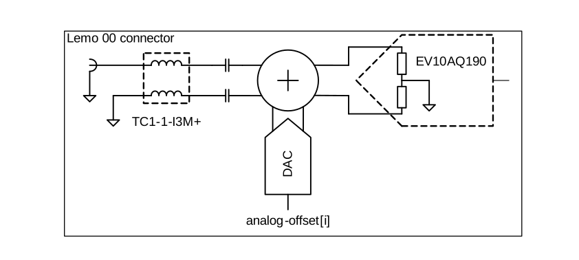
Figure 4 Input circuit for each of the four analog channels A to D.
Analog Offsets
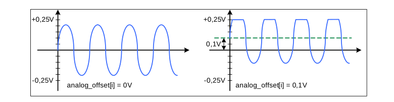
Figure 5 User-defined analog offset to the input before sampling.
AC coupling removes the common mode voltage (DC voltage) from the input signal.
Users can move the common mode voltage to a value of their choice using the
ndigo_configuration::analog_offset
parameter of each channel before sampling.
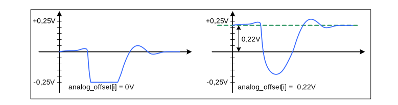
Figure 6 Highlight how the user defined offset increases dynamic range for asymmetric input pulses.
This feature is useful for highly asymmetric signals (see Figure 6), such as pulses from TOF spectrometers or LIDAR systems. Without analog offset compensation, the pulses would begin in the middle of the ADC range, effectively cutting the dynamic range in half. By shifting the common mode voltage to one end of the ADC range, the input range can be fully utilized, providing the maximum dynamic range.
The analog offset can be set between ±0.25 V.
Attention
After calling ndigo_init(), the ADC chip will heat up,
which will slightly shift its baseline.
If you plan to measure very small pulses, wait for about 2 minutes after
calling ndigo_init before you start capturing data and set the values
of analog_offset only after this startup
period.
Digital Inputs
There are two digital inputs on the front slot cover called Trigger and Gate.
Both inputs provide a digital input signal routed to the trigger matrix.
These signals can be used to trigger any of the trigger state machines
and gating blocks.
The inputs are AC coupled. DC offset is configurable via
ndigo_configuration::dc_offset to support
positive and negative input pulses.
The digital inputs are further configured using
ndigo_configuration::trigger
Figure 17 in Trigger Blocks shows the trigger units of the digital channels.
TDC on Trigger Input
There is a time-to-digital converter connected to the Trigger input.
When used with the TDC, the Trigger input supports negative pulses only.
For TDC data, the output packets (see Output Data Format) will
have type equal to
NDIGO_PACKET_TYPE_TDC_DATA.
These packets first contain a coarse timestamp and a payload that can be used
to calculate the trigger position with higher precision.
The function ndigo_process_tdc_packet() can be used to replace
the coarse timestamp with the precise timestamp.
TDC pulses must have a minimum duration of 3.3 ns.
The dead-time of the TDC is 32 ns.
Extension Card
The Ndigo Extension Card provides additional inputs or outputs to the Ndigo5G board. It is connected to the Samtec QSS-025 connector on an Ndigo5G by a Samtec SQCD cable assembly.
The Ndigo Extension Card provides up to ten single ended LEMO00 connectors.
The circuit connecting to each of these circuits can be chosen to provide inputs or outputs.
These can be AC or DC coupled. AC-coupled inputs support NIM signaling.
The signals connect to 2.5 V IO pins of the Xilinx Virtex-5 FPGA present on the Ndigo5G board.
The current firmware revision provides the following signal connections.
Connector |
QSS Pin |
FPGA Pin |
Direction |
Signal |
|---|---|---|---|---|
LEMO00: CH0 |
22 |
AD9 |
Input |
Ndigo Extension digital channel 0 |
LEMO00: CH1 |
18 |
AE10 |
Input |
Ndigo Extension digital channel 1 |
LEMO00: CH2 |
14 |
D10 |
not connected |
|
LEMO00: CH3 |
10 |
AF9 |
Output |
39.0625 MHz clock for HPTDC |
LEMO00: CH4 |
6 |
AD11 |
Output |
39.0625 MHz clock for HPTDC |
LEMO00: CH5 |
5 |
AE7 |
Output |
39.0625 MHz clock for HPTDC |
LEMO00: CH6 |
9 |
AF7 |
Output |
39.0625 MHz clock for HPTDC |
LEMO00: CH7 |
13 |
D9 |
not connected |
|
LEMO00: CH8 |
17 |
V9 |
Input |
Ndigo Extension digital channel 2 |
LEMO00: CH9 |
21 |
W9 |
Input |
Ndigo Extension digital channel 3 |
SYNC1: Sync-TDC8 |
26 |
F9 |
not connected |
|
SYNC1: Sync-HPTDC |
44 |
AA7 |
Output |
Sync for HPTDC |
The four digital inputs are routed to the bus inputs of the trigger matrix and can be used for triggering.
The routing can be configured to either OR-ing the sync bus and extension channels or to use the extension channels exclusively.
Connector |
Extension Card |
Trigger matrix input |
Trigger matrix input |
|---|---|---|---|
Digital Channel |
ignorecable = 0 |
ignorecable = 1 |
|
LEMO00: CH0 |
0 |
BUS0 = EXT0 Sync Cable 0 |
BUS0 = EXT0 |
LEMO00: CH1 |
1 |
BUS1 = EXT1 Sync Cable 1 |
BUS1 = EXT1 |
LEMO00: CH8 |
2 |
BUS2 = EXT2 Sync Cable 2 |
BUS2 = EXT2 |
LEMO00: CH9 |
3 |
BUS3 = EXT3 Sync Cable 3 |
BUS3 = EXT3 |