Hardware
The xTDC4 is available as a PCIe plugin board (variant “–PCIe”) or as a desktop solution (variant “–TBT”). The two variants are shown in Figure 1.
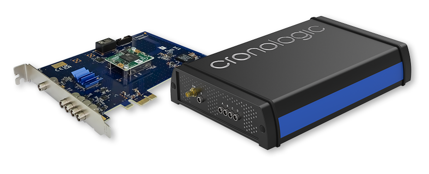
Figure 1 Overview of the PCIe (left) and the TBT (right) variant of the xTDC4.
Installing the PCIe Board
The xTDC4 board can be installed in any PCIe-CEM slot with x1 or more lanes. Make sure that the PC is powered off and the main power connector is disconnected while installing the board.
Input and Connectors
Figure 2 shows the location on the inputs on the slot bracket. Figure 3 shows a side view of the PCIe variant of the xTDC4.

Figure 2 Input connectors of the xTDC4 on the PCIe bracket.

Figure 3 Schematic of the xTDC4 PCIe board. The connectors J12 and J25 are only present on Gen 1 boards.
LEMO-00 connectors are used for input connection. The inputs are AC-coupled and have an impedance of 50 Ω. A schematic of the input circuit is shown in Figure 4.

Figure 4 Input circuit of the TDC channels.
The digital threshold for each input can be adjusted individually to comply with a
multitude of single-ended signaling standards
(see xtdc4_configuration.dc_offset). The threshold can also be used
to configure the input for either positive or negative pulses.
The connectors can also be used as outputs. DC-coupled output pulses for automatic internal triggering and control of external devices can be generated using the Timing Generators (TiGer).
The SMA connector at the top edge of the board can be used to connect an external
10 MHz clock signal. To enable use of an external clock, configure
xtdc4_init_parameters.use_ext_clock accordingly.
Only Gen 1 xTDC4 boards have inter-board connectors near the top edge of the board. The pinout of connector J12 is shown in Table 1. The connector J12 is reserved for future use.
Pin |
Name |
|---|---|
1, 2 |
GND |
3, 4 |
external CLK in N, external CLK in P |
5, 6 |
GND |
7, 8 |
reserved/NC |
9, 10 |
GND |
11, 12 |
reserved/NC |
13, 14 |
GND |
15, 16 |
reserved/NC |
17, 18 |
GND |
19, 20 |
reserved/NC |
21, 22 |
GND |
23, 24 |
reserved/NC |
25, 26 |
GND |
27, 28 |
reserved/NC |
29, 30 |
GND |
31, 32 |
reserved/NC |
33, 34 |
GND |
Status LEDs of the PCIe boards
Note
This section refers to the status LEDs of the PCIe board, not the LEDs of the TBT variant (see here).
Three status LEDs are present on the board, as seen in Figure 3.
LED1 lights up red during the configuration of the FPGA and turns off afterward. If it stays permanently lit, the configuration failed.
LED2 lights up green after the board is initialized by the driver and turns off when the device is closed by the software.
LED3 lights up green when capture is started, yellow after the first start signal was detected and red when groups are missing.
Memory Management
The xTDC4 has internal FIFOs (first-in, first-out) that buffer data during acquisition.
The data is streamed from the internal FIFOs to the host PC and stored in the host buffer. Data will only be overwritten in the host buffer if it has been acknowledged.
The host buffer is managed by the DMA (direct memory access) driver. The DMA driver can only ever write to the host buffer if enough memory is free. That means, new packets will never overwrite old packets unless they have been acknowledged.
If the host buffer is full, data may be lost. If this occurred, the corresponding
packets will have the
XTDC4_PACKET_FLAG_HOST_BUFFER_FULL
bit of crono_packet.flags set. This may result in lost packets.
If the hit rate is too high, the internal FIFOs may fill up. If this is the case,
the affected packets will have the
XTDC4_PACKET_FLAG_DMA_FIFO_FULL
bit of crono_packet.flags will be set. This may result in lost packets.
However, only if the
XTDC4_PACKET_FLAG_SHORTENED
bit of crono_packet.flags is set, packets were actually missed.