1 Hardware
1.1 Overview
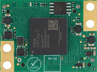
Figure 1.1: Top-view of a TimeTagger Module.
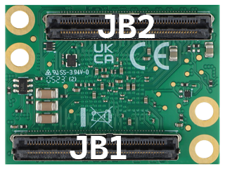
Figure 1.2: Bottom-view of a TimeTagger Module. For the pin assignment of connectors JB1 and JB2, see Section 1.5. In the above image, Pin 1 is at the bottom right of the connectors, respectively.
Figures 1.1 and 1.2 show the top and bottom view of the module.
The TimeTagger Module is connected to a carrier board using two B2B connectors Samtec Razor BeamTM LSHM-150 (JB1, JB2). Figure 1.3 shows the dimensions of the board as well as the positioning of the two B2B connectors.
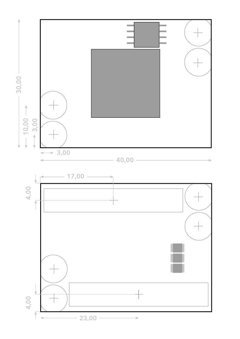
Figure 1.3: Dimensions of the module and placement of the B2B connectors and mounting holes. All dimensions are in mm. Mating height with a standard connector is 8 mm.
Figure 1.4 shows the principle of how the TimeTagger Module may be implemented on a PCIe carrier board. Note that it only gives an overview of a possible setup. Details for the implementation are given in the sections below.
The PCIe 12 V supply a PSU with regulated 3.3 and 2.5 V outputs supplying the TimeTagger Module with power.
The TimeTagger Module communicates with the computer via PCIe.
A 150 MHz oscillator is connected to the module.
The COAX start and stop signals are discriminated and connected to the module.
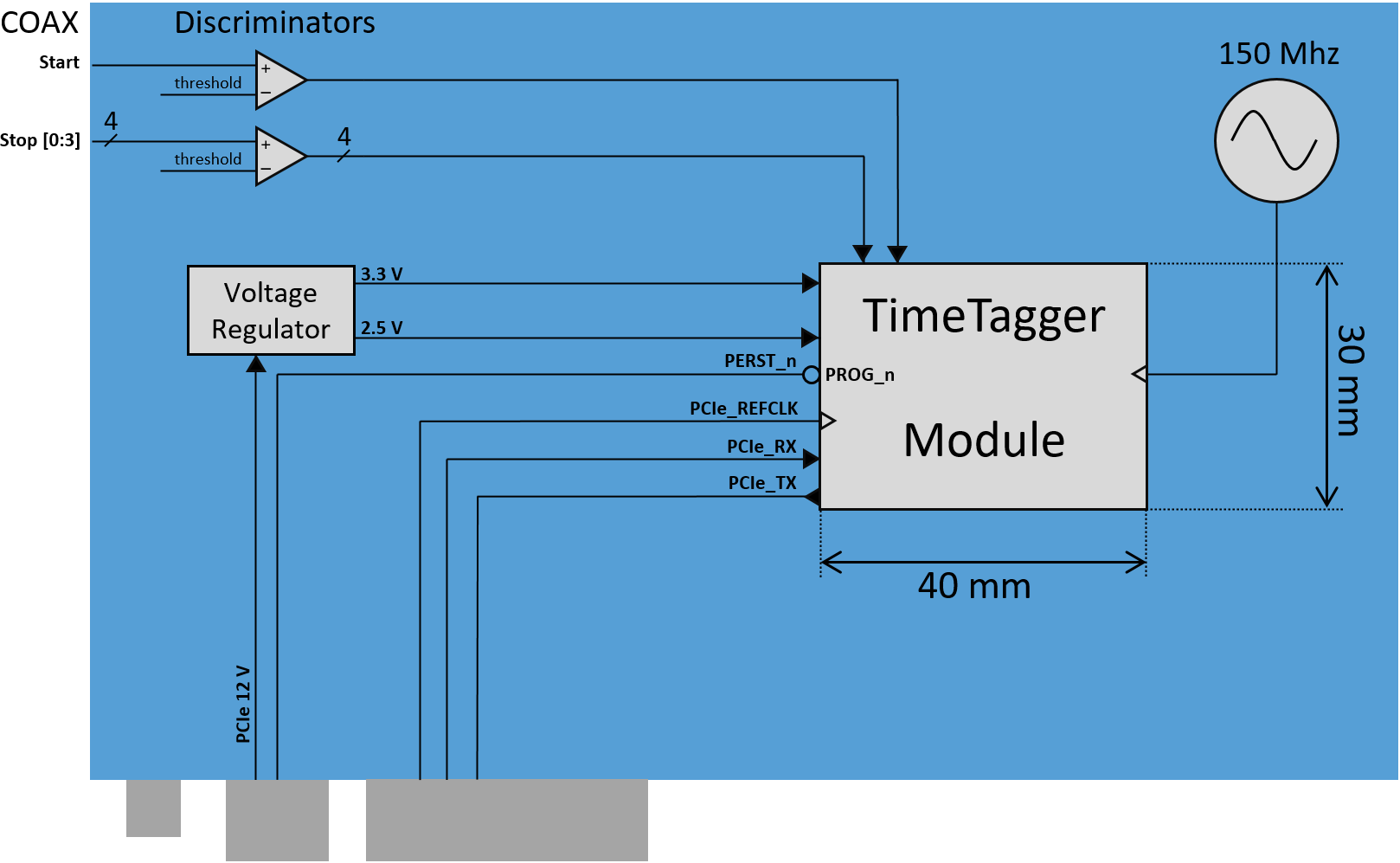
Figure 1.4: Example setup of a TimeTagger Module on a PCIe board.
1.2 Inputs and Outputs
Figure 1.5 gives an overview of the required and optional input and output signals of the TimeTagger Module. The required standards are listed in Section 1.4.

Figure 1.5: Block diagram giving an overview of the inputs and outputs of the TimeTagger Module, respectively.
1.2.1 Supply Voltages
VCC33 and VCC25
Supply voltages of 3.3 V and 2.5 V.
1.2.2 Clocking
PCIe_100M_CLK
A differential 100 MHz clock that complies with PCIe clock specifications with regard to signaling levels and jitter.
This must be synchronous to the clock of the PCIe host connected to the module. It can be taken directly from the clock of a PCIe_CEM connector.
100 nF decoupling capacitors should be placed in series of this signal to implement AC coupling.
TDC_150M_CLK
A differential LVDS clock signal with 150 MHz frequency. This can be either synchronous or asynchronous to PCIe_100M_CLK.
The quality of this clock effects the measurement accuracy of the TDC, so a low-jitter clock source must be used. Spread-spectrum clocking should be disabled for this signal.
1.2.3 Main Signals
All these signals must be correctly connected to operate the TimeTagger Module.
PROG_b
3.3 V CMOS input.
Strobe LOW to initiate a reload of the FPGA firmware.
In a PCIe-CEM system this should be connected to the PERST_b pin of the connector and provided with a 5 kΩ pull-up to 3.3 V. When connected to 3.3 V, the firmware is only loaded once at power-up.
PERST_b
3.3 V CMOS input.
Reset the PCIe core of the FPGA.
In a PCIe_CEM system, this should be connected to the corresponding signal from the edge connector. In an embedded system the requirements can vary, but it could be controlled by a microcontroller output.
Timing should comply to the PCIe_CEM specification.
PCIe_TX[3:0]
Differential PCIe output signals to transmit packets from the TimeTagger Module to the host. Compliant to PCIe standards. The _P and _N signals of each pair can be flipped to simplify routing.
The PCIe protocol will detect and correct the inversion.
Lanes 0 to 3, or lanes 0 and 1, or only lane 0 can be connected to the host. The ordering of lanes can be reversed to simplify routing.
PCIe_RX[3:0]
Same as PCIe_TX but an input for receiving packets from the host at the module. 100 nF decoupling capacitors must be placed in series to these signals.
START
Differential LVDS input to start a TDC measurement. If single ended signals or small scale signals shall be processed, a discriminator must be implemented.
This signal must not be left floating and should always be in a well-defined LOW or HIGH state.
STOP[3:0]
Differential LVDS input to create a time measurement on the respective channel.
This signal must not be left floating and should always be in a well-defined LOW or HIGH state.
1.2.4 Optional Signals
These signals are not necessary for operating the module, but they can provide useful additional features.
Attention
Even if not in use, JTAG_TCK and TEMP_ALARM_b have to be connected correctly. See the descriptions of these signals for details.
JTAG signals
The JTAG port for debugging, re-flashing and interactive development of the FPGA hardware. This is usually not required for a production system, as the firmware delivered with the module provides the capability to update the firmware over PCIe.
However, we recommend implementing a JTAG connector anyway if space is available, to simplify debugging of the base board. See Figure 1.6 for the implementation.
There are various JTAG cables for FPGA development available. The following circuit is compatible to the JTAG-HS2 Programming Cable by Digilent, provided, e.g., by trenz electronic.
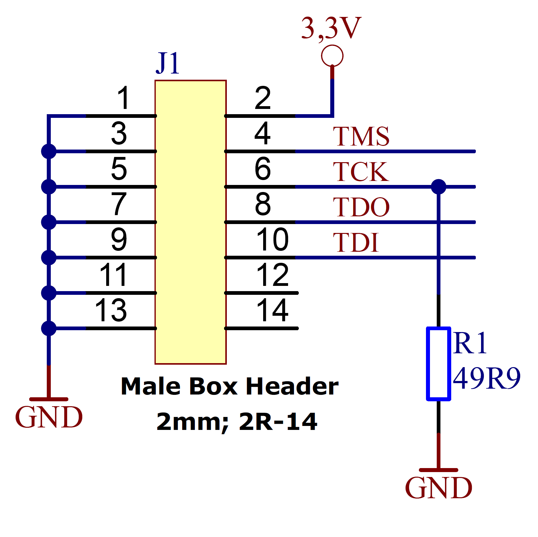
Figure 1.6: Circuit diagram for a JTAG connector.
- JTAG_TDI
3.3 V CMOS input.
Data from the JTAG controller to the FPGA.
- JTAG_TDO
3.3 V CMOS output.
Data from the FPGA to the JTAG controller.
- JTAG_TMS
3.3 V CMOS input.
Control signal from the JTAG controller to the FPGA.
- JTAG_TCK
3.3 V CMOS input.
Clock signal from the JTAG controller to the FPGA.
If JTAG is used, a 50 Ω termination close to the FPGA module is required.
Otherwise, if JTAG is not used, this signal must be tied to GND or 3.3 V.
Status Signals
There are four signals provided that can be used to provide information about the module status.
In the original TimeTagger4 base boards, these signals are connected to LEDs to provide visual feedback to the user. In an embedded system they could alternatively be connected to microcontroller inputs.
- DONE
3.3 V CMOS output.
A high value indicates that the FPGA completed configuration. cronologic usually connects this to a red LED over a 220 Ω series resistor.
The LED is lighting up during configuration so that a failed configuration is immediately visible.
- STAT_INITIALIZED
3.3 V CMOS output.
Is set to HIGH after the board is initialized by the driver.
Is reset to LOW when the device is closed by the software.
- STAT_CAPTURE[1:0]
3.3 V CMOS output.
Provide status information. These can be connected to 3.3 V via 120 Ω series resistor and an LED.
STAT_CAPTURE[0] is set HIGH when the driver is in the capturing state.
Then, STAT_CAPTURE[1] becomes HIGH when a first start pulse is detected during capturing.
These bits are sticky and stay HIGH until capturing is stopped, with one exception: If missing groups are detected, STAT_CAPTURE[0] becomes LOW and STAT_CAPTURE[1] becomes HIGH.
These pins can be connected to a dual-color LED that lights up, e.g., green when capture is started, yellow when start signals are detected, and red when groups are missing. For this STAT_CAPTURE[0] should light up the green LED and STAT_CAPTURE[1] should light up the red LED.
TiGer Signals
- TiGer[4:0]
3.3 V CMOS output.
These pins are controlled by the TiGer timing generator. They can be used to control the timing of the system with high precision.
- TiGer_OE[4:0]
3.3 V CMOS output. Output Enable for the TiGer.
On cronologic’s TimeTagger4 boards, the connectors for the TiGer outputs are shared with the TDC inputs.
To facilitate this, tri-state buffers close to the connector are used to conditionally drive the TiGer signals to the connector.
The buffers are enabled when TiGer_OE is HIGH. In an embedded system the TiGer signals usually can be routed directly to their sinks and the output enables can be left unconnected.
DAC Control
The driver for the module supports controlling of two DAC8565 digital-to-analog converters to configure the input thresholds of the discriminators and the oscillator control voltage.
In an embedded system, the same setup can be used. Alternatively, the voltages can be controlled by a microcontroller or set to fixed voltages.
DAC1 has OSC_VC on VOUTA and the discriminator threshold of the START input on VOUTD.
DAC2 has the discriminator thresholds of the for stop channels on its VOUTx outputs.
DAC3 is not supported yet. The enable is provided to allow future versions with more channels.
It is possible to change the meaning of the voltages. For example, VOUTD of DAC1 can be used as a common threshold for all inputs. But the driver will not know that and this voltage will be accessed by the user as the START channel threshold.
- DAC_SYNC
3.3 V CMOS output.
Connect to the SYNC_b pins of the DACs. Avoid stubs.
- DAC_SCLK
3.3 V CMOS output.
Connect to the SCLK pins of the DACs. Avoid stubs.
- DAC_D
3.3 V CMOS output.
Connect to the DIN pins of the DACs. Avoid stubs.
- DAC_RST_b
3.3 V CMOS output.
Connect to the RST_b pins of the DACs. Avoid stubs.
- DAC_EN
3.3 V CMOS output.
Connect to the ENABLE_b pin of the DAC with the same index.
BOARD[3:0]
3.3 V CMOS output.
A bit pattern of 4 bits that is made visible in the driver API.
Can be used to communicate version or type information about the base board to the software, in case it has to act differently for certain variants.
TEMP_ALARM_b
3.3 V CMOS input.
When set to LOW, the driver will report a temperature alarm. Can be connected to the alarm output of a temperature sensor, to a microcontroller, or can be connected to 3.3 V.
POWON
3.3 V CMOS output.
This signal is set to HIGH after all power supplies of the module are stable and the FPGA on the module is configured.
It can be used to enable power supply circuits that are not required to supply the TDC module.
1.3 Routing of Differential Signals
All differential signals on the board are high speed signals that must be routed carefully to provide good signal integrity.
The routing can either be done as a coupled pair with 100 Ω differential impedance or as two independent wires with 50 Ω single ended impedance.
An uninterrupted reference plane should be on the next layer along the whole stretch of the connection. Stubs and branches must be avoided.
All differential inputs are terminated on the board with 100 Ω differential termination.
1.4 Signal Standards
The superscript next to the signal names of the tables in Sections 1.5.1 and 1.5.2 refer to the signal standard, as listed below.
- 1PCIe
Differential signals with an impedance of 100 Ω compliant with the PCIe_CEM standard.
- 2LVCMOS33
For input signals, VIL and VIH specify the input voltage for LOW and HIGH, respectively.
For output signals, VOL and VOH specify the output voltage of LOW and HIGH, respectively.
VIL,min |
VIL,max |
VIH,max |
VIH,max |
VOL,max |
VOH,min |
IOL,max |
IOH,min |
|---|---|---|---|---|---|---|---|
−0.3 V |
0.8 V |
2.0 V |
3.45 V |
0.4 V |
2.9 V |
11 mA |
−11 mA |
- 3LVDS
In the table below, VIDIFF is the differential input voltage (U − Ū), where U is HIGH [or (Ū − U), where Ū is HIGH]. VICM is the input common-mode voltage. The input impedance is 100 Ω differential.
Symbol |
Min |
Typical |
Max |
Unit |
|---|---|---|---|---|
VIDIFF |
100 |
350 |
600 |
mV |
VICM |
0.3 |
1.2 |
1.5 |
V |
- 4VCC33
min. 3.2 V; max 3.4 V
- 5VCC25
min. 2.4 V; max 2.6 V
1.5 Pin Assignment
The tables in Sections 1.5.1 and 1.5.2 list the pin assignments of connectors JB1 and JB2 (see Figure 1.2).
Some signals are optional and do not have to be connected, as is described in Section 1.2.
Pins that must not be connected are marked as NC.
1.5.1 Connector JB1
Pin assignment of the JB1 connector. The superscripts refer to the signal standard (see Section 1.4)
Name |
Pin |
Pin |
Name |
Name |
Pin |
Pin |
Name |
|
|---|---|---|---|---|---|---|---|---|
1 |
2 |
NC |
51 |
52 |
NC |
|||
3 |
4 |
NC |
53 |
54 |
||||
GND |
5 |
6 |
GND |
NC |
55 |
56 |
||
7 |
8 |
NC |
57 |
58 |
||||
9 |
10 |
NC |
59 |
60 |
||||
GND |
11 |
12 |
GND |
Connect to JB1-83 |
61 |
62 |
||
13 |
14 |
63 |
64 |
|||||
15 |
16 |
65 |
66 |
GND |
||||
GND |
17 |
18 |
GND |
67 |
68 |
NC |
||
19 |
20 |
69 |
70 |
NC |
||||
21 |
22 |
NC |
71 |
72 |
NC |
|||
GND |
23 |
24 |
GND |
NC |
73 |
74 |
NC |
|
NC |
25 |
26 |
NC |
75 |
76 |
NC |
||
GND |
27 |
28 |
NC |
77 |
78 |
NC |
||
GND |
29 |
30 |
GND |
NC |
79 |
80 |
NC |
|
GND |
31 |
32 |
NC |
81 |
82 |
|||
GND |
33 |
34 |
Connect to JB1-61 |
83 |
84 |
GND |
||
NC |
35 |
36 |
NC |
85 |
86 |
|||
GND |
37 |
38 |
NC |
87 |
88 |
|||
39 |
40 |
NC |
89 |
90 |
||||
41 |
42 |
NC |
91 |
92 |
||||
43 |
44 |
NC |
NC |
93 |
94 |
|||
45 |
46 |
NC |
NC |
95 |
96 |
DONE2 |
||
GND |
47 |
48 |
GND |
97 |
98 |
GND |
||
49 |
50 |
NC |
99 |
100 |
GND |
|||
GND |
F1 |
F2 |
GND |
1.5.2 Connector JB2
Pin assignment of the JB1 connector. The superscripts refer to the signal standard (see Section 1.4)
Name |
Pin |
Pin |
Name |
Name |
Pin |
Pin |
Name |
|
|---|---|---|---|---|---|---|---|---|
NC |
1 |
2 |
NC |
51 |
52 |
NC |
||
NC |
3 |
4 |
NC |
NC |
53 |
54 |
||
NC |
5 |
6 |
NC |
NC |
55 |
56 |
||
NC |
7 |
8 |
NC |
57 |
58 |
|||
NC |
9 |
10 |
59 |
60 |
NC |
|||
NC |
11 |
12 |
NC |
61 |
62 |
NC |
||
NC |
13 |
14 |
GND |
63 |
64 |
NC |
||
NC |
15 |
16 |
NC |
65 |
66 |
NC |
||
GND |
17 |
18 |
NC |
NC |
67 |
68 |
NC |
|
NC |
19 |
20 |
NC |
NC |
69 |
70 |
NC |
|
NC |
21 |
22 |
NC |
NC |
71 |
72 |
GND |
|
NC |
23 |
24 |
NC |
NC |
73 |
74 |
NC |
|
NC |
25 |
26 |
NC |
NC |
75 |
76 |
NC |
|
NC |
27 |
28 |
NC |
NC |
77 |
78 |
NC |
|
NC |
29 |
30 |
NC |
NC |
79 |
80 |
NC |
|
NC |
31 |
32 |
NC |
81 |
82 |
NC |
||
NC |
33 |
34 |
GND |
83 |
84 |
NC |
||
GND |
35 |
36 |
GND |
NC |
85 |
86 |
NC |
|
NC |
37 |
38 |
NC |
NC |
87 |
88 |
NC |
|
NC |
39 |
40 |
NC |
NC |
89 |
90 |
GND |
|
41 |
42 |
NC |
NC |
91 |
92 |
NC |
||
43 |
44 |
NC |
NC |
93 |
94 |
NC |
||
45 |
46 |
NC |
NC |
95 |
96 |
NC |
||
47 |
48 |
NC |
NC |
97 |
98 |
NC |
||
49 |
50 |
NC |
NC |
99 |
100 |
NC |
||
GND |
F1 |
F2 |
GND |